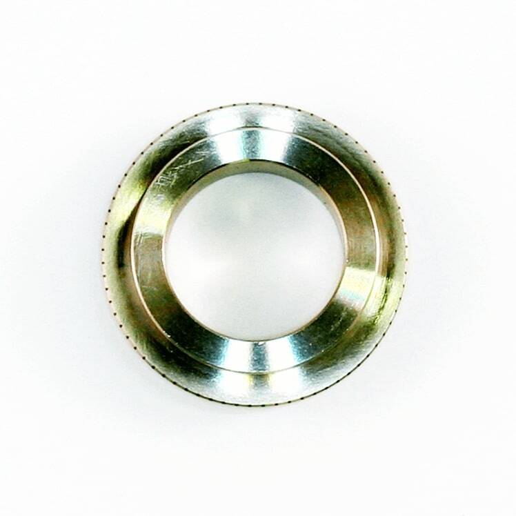
BF RMS W20.32 x 0.706, 45 mm
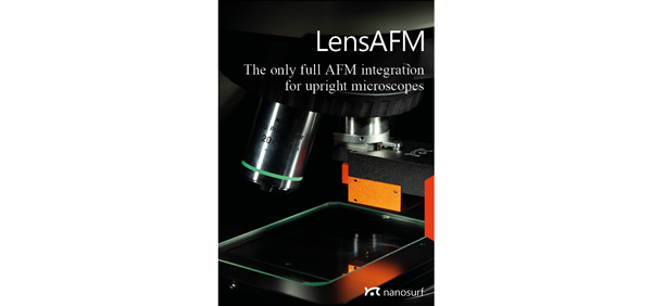
The Nanosurf LensAFM is an atomic force microscope that picks up where optical microscopes and profilometers reach their resolution limits. It is mounted like a normal objective lens, thus extending the resolution and measuring capabilities of these instruments. The LensAFM not only provides 3D surface topography information, but can also be used to analyze various physical properties of a measurement sample.
Speak with an expert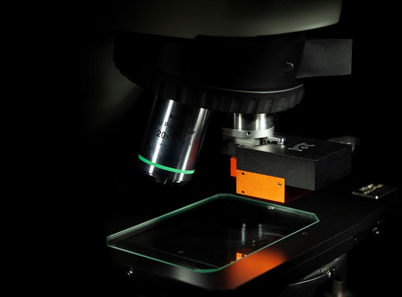
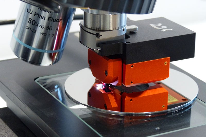
In an ever-increasing number of situations, researchers are looking to combine optical and atomic force microscopy techniques. The ease of use, screening capability, and minimal sample preparation requirements of optical microscopes are almost unparalleled. However, when the resolution of a 100x objective is not sufficient to examine small features beyond the instrument's resolution, the LensAFM comes into play. Its exceptionally small design and clever mounting mechanism mean you only need to rotate the turret on your optical microscope or profilometer and run the scan.
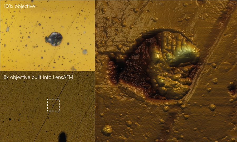
Since the resolution of optical microscopy is limited by the wavelength of light, there is a barrier in the resolution you can achieve with your optical system. In an ever-increasing number of applications, this calls for the combination of optical and atomic force microscopy. In addition, AFM overcomes problems characterizing transparent samples or samples otherwise difficult to assess optically. But not only the coarse topography of a sample is of interest: AFM also allows knowledge of other material properties to be acquired, e.g. surface roughness, hardness variations, magnetism, or electrical conductance/resistance.
Image: Optical images (left) and AFM topography image (right) of a defect in a hard-coated metal surface.
The LensAFM not only enhances the precision of measurements but also saves time. Thanks to the alignment grooves, there's no need to perform a laser alignment on the cantilever, which streamlines the process and saves additional time. This makes the LensAFM an invaluable tool in any research setting that requires the detailed analysis provided by atomic force microscopy.
The LensAFM integrates perfectly into your existing workflow. Once mounted on your optical microscope's turret – just like a regular objective lens – you can screen the sample with optical methods to find areas of interest. Subsequently, these areas of interest are easily found again using the integrated 8x optical lens, and then you can perform your AFM measurement for higher resolution 3D information. This approach allows you to work in the way you are used to but with a significant boost in resolution and capabilities.
.jpg?width=2000&name=LensAFM%20on%20Zeiss%20(mounting).jpg)
"The unique combination of compact design, optical access, and intuitive operation of the LensAFM made it the perfect platform for our instrument development. We believe that much of the success of our project has been achieved through the excellent communication that we have enjoyed between ourselves, Nanosurf, their UK distributor Windsor Scientific, and AFM probe manufacturer Nanosensors. We now look forward to future developments with the LensAFM to optically probe magnetic materials deep into the nanoscale."

BF RMS W20.32 x 0.706, 45 mm

DF M27 x 0.75, 45 mm

DF RMS W26x0.706, 45mm

M25x0.75, 45 mm

M25x0.75, 60 mm

M32x0.75, 45 mm

M32x0.75, 60 mm

RMS W26x0.706, 95 mm
The PDF brochure includes details on the LensAFM's technology, application examples for different areas of interest and system specifications.
#{ row.name }
#{ item.resourceType }
#{ item.date_text_field }
#{ truncateText(item.metadescription) }
#{ item.readmoretext }Get to know the LensAFM! Reach out to us to discuss your application with one of our seasoned AFM experts, to get a budgetary quote or schedule a product demonstration or exploratory meeting.