Conductive Atomic Force Microscopy (C-AFM)
Conductive AFM uses a sharp conductive probe to map local variations in a sample’s conductivity with nanoscale resolution. The method of conductive force microscopy or C-AFM described here is an electrical mode in the SPM family. It is used to study a sample’s conductivity and image electrical properties such as charge transport and charge distribution on the nanoscale. C-AFM is applied in the nanoelectronics field, solar cell and semiconductor industries for a wide variety of high resolution measurements including semiconductor dopant profiling and quality control for dielectric films and oxide layers.
In conductive AFM, a sharp conductive tip is in contact with the sample. During this contact, a bias voltage is applied between afm tip and sample and the current flow is measured between the two as the probe raster scans across the surface, creating a conductivity or current map. This mode is similar to scanning tunnelling microscopy (STM), which was the original SPM technique. C-AFM offers a key advantage over STM because C-AFM uses a conductive cantilever instead of a sharp metallic wire. Additionally, C-AFM images topography through the optical beam deflection detector system used in all AFM measurements. The electrical conductivity is measured with a low noise, high gain preamplifier. With this setup, topography and current information are collected independently in C-AFM (unlike STM where the topography and current image are dependent on one another), which minimizes convolution of the two signals and artifacts as well as simplifying the interpretation of the acquired conductivity and current maps.
The conducting probe in C-AFM has a thin conducting coating. Common electrically conducting coatings are platinum, gold, tungsten, and conductive diamond. These cantilevers are inexpensive and commercially available.
C-AFM operates in contact mode. In this mode, the tip is in constant contact with the sample. The load exerted by the tip on the sample is set by the user and monitored through the cantilever deflection. The probe then raster scans along the surface using a feedback loop to keep this cantilever deflection constant through z piezo motion. This mode of operation can lead to a fairly aggressive tip-sample interaction that can wear the tip quickly. Combined with the high current densities flowing through the tip/sample contact, C-AFM probes can wear out faster than silicon based probes used for conventional SPM topography measurements.
Current measurements with conductive AFM in air can be challenging. The contact area between tip and sample is very small (diameter in the 10nm range) leading quickly to high current density (current per surface area unit), rapidly deteriorating the conductive properties of the cantilever coating. A resistor inline with the sample reduces this risk of highly conductive samples.
Surface contamination and a water film between tip and sample commonly present at ambient conditions can also reduce reliability and repeatability of C-AFM. Only a few nanometers of debris on the tip can block the flow of electrical current. Therefore higher forces are sometimes needed, which require harder tip materials or coatings like conductive diamond-like coatings or platinum silicide since these higher forces will degrade the tip faster.
Finally, localized single point measurements of current-voltage (I-V) curves can also be collected with C-AFM. For these electrical measurements, the user places the probe at the desired location on the sample surface and ramps the bias voltage while collecting the current.
Examples of C-AFM
Below is a 500nm x 500nm C-AFM image of an HOPG surface where the z range is only 80 pA. The different conductivities (dark and bright red) of the different layers in the HOPG can be easily observed in the contrast of the low current image.
Low current cAFM measurement on HOPG. 500nm x 500nm; z-range 80pA
Another example of the application of C-AFM comes from the catalyst material industry. Fuels cells with cathode catalysts layers consist of platinum nanoparticles embedded in a carbon matrix. The electron transport is dominated by electron tunneling between neighboring platinum particles so that the platinum particle density governs the conducting or insulating nature of the cathode layer.
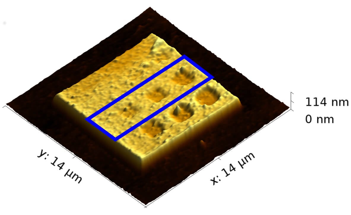
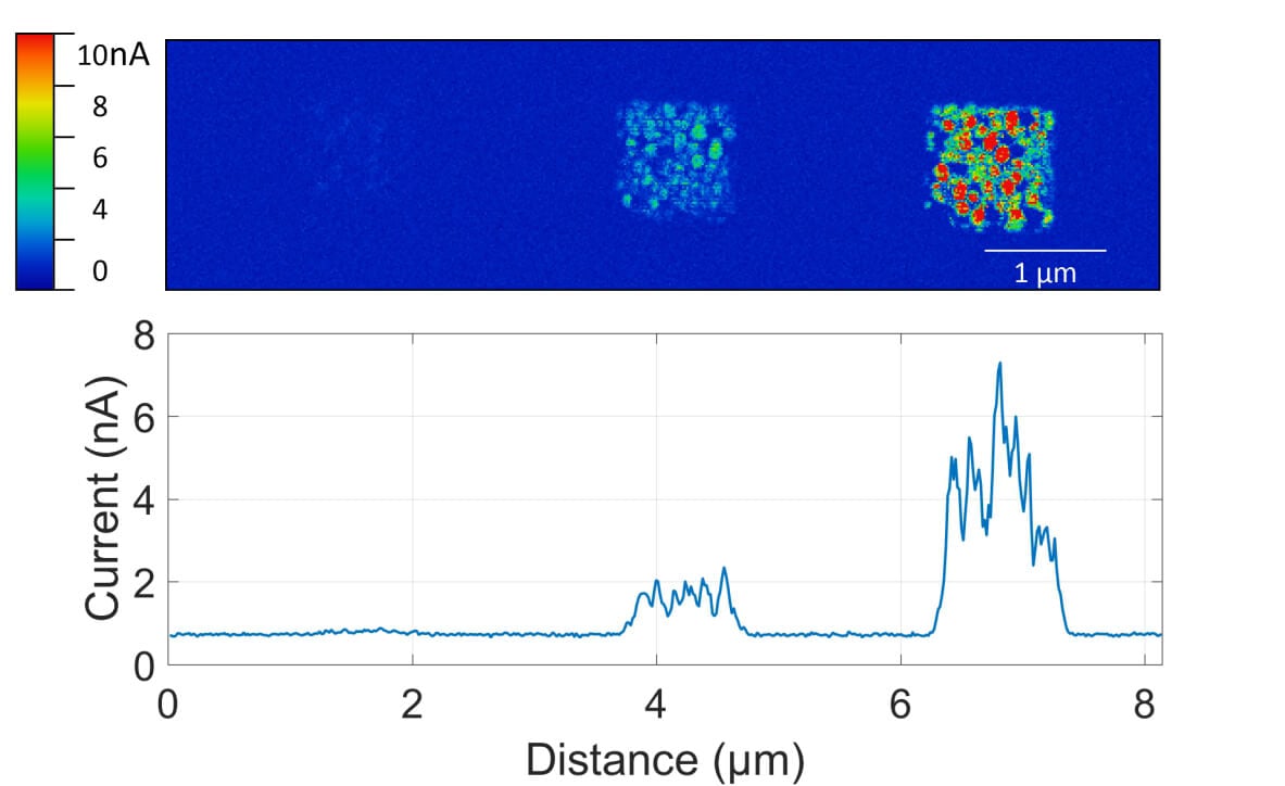
In this example, C-AFM monitored changes in conductivity of the carbon matrix layer as it was irradiated by an electron beam. The irradiation oxidized the carbon, making the matrix more compact and reducing the distance between the platinum nanoparticles. The AFM topography image shows different spots of electron beam irradiation where the topographic depressions show the compacting of the film at these points. Simultaneous with the topography, the conductivity at each of these points is measured with C-AFM as shown below. Higher film compaction spots with higher irradiation dose on the right of the image (i.e. more topographic depression) corresponds to increased local conductivity in these areas.

3D topography of Pt(C) thin film irradiated with different electron beam doses

Current through the film of the area inside the blue rectangle in the topography