Discover how Nanosurf's industrial automated AFM systems are developed from concept to delivery, ensuring precise ...

17.05.2024

Héctor here, your AFM expert at Nanosurf calling out for people to share their Friday afternoon experiments. Today, with some help from Denis Vasyukov and the SSRM module, I image the transistors on a mobile phone CPU.
Today's fridayAFM took one friday afternoon to do the AFM measurements, and several weeks of sample preparation (for which I have to thanks Denis Vasyukov who took care of doing all that preparation for me).
What we imaged? The finFET transistors on a mobile phone CPU (Samsung Samsung Exynos 8895 with 10 nm technology node).
Sample preparation required chip decapping with chemicals and cutting and polishing the cross section of the chip with focused ion beam (FIB).
AFM measurements where performed with the SSRM module to measure conductivity.
Here is the video summarizing it all:
Let's recap. We took the CPU from a phone and cut it in half using FIB to polish the exposed cross section. Then we measured conductivity using the SSRM module, which, with the help of some literature research, allowed us to identify the finFET structures.
I hope you find this useful, entertaining, and try it yourselves. Please let me know if you use some of this, and as usual, if you have suggestions or requests, don't hesitate to contact me.
Further reading:
New White Paper: Unveiling the Power of Electrical Modes
https://semiconductorian.wordpress.com/2021/08/06/giai-phau-bong-ban-dan-fet/
Extra:
For those with no time to go through the video.
We took a commercial smartphone and break it a part.

Then we extracted the CPU and removed the encapsulation using H2SO4.

Next, we used focused ion beam to cut the chip and have a polished cross-section.

Then using silver paste and a metal disc, the sample was mounted vertically to be able to image the edge.

The render of how we are going to image is something like this:

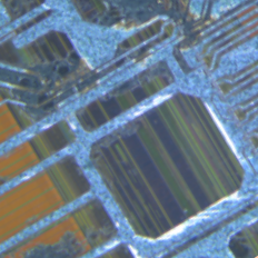
and the actual optical microscope view is this:

The different colors in the render indicate materials with different conductivity, and to measure conductivity we used scanning spreading resistance microscopy (SSRM), which is a type of conductive AFM that uses a logarithmic amplifier to measure conduction and be able to distinguish details between areas with high/low conductivity.

Next we capture the conductivity maps in Static mode with a DriveAFM.


The topography was hard to interpret

But the conductivity map was more straightforward. basically we were looking at some interconnections with high conductivity, some insulating parts, and the fine smaller details were likely transistors.

Doing some literature research online, it is very likely that the small features were FinFET transistors.

Probably two of them in the same orientation as they are represented in the Wiki article.
So, in summary. We demonstrate that measuring cross sections of integrated circuits is possible, and that SSRM has enough spatial and conductivity resolution to visualize FinFET devices.
25.02.2026
Discover how Nanosurf's industrial automated AFM systems are developed from concept to delivery, ensuring precise ...

10.02.2026
High-end industrial solution are powered by accurate software that coordinate all their functions. Discover the ...

20.01.2026
Read how Nanosurf designs AFM stages to meet industrial challenges, ensuring precision and stability in AFM systems for ...

08.12.2024
Learn how to make a Python code to interface your AFM with a gamepad.

01.10.2024
Discover how different types of glass age and degrade over time, and learn how to use AFM technology to investigate ...
11.07.2024
FridayAFM: learn how to perform datamining on large sets of AFM data.
Interested in learning more? If you have any questions, please reach out to us, and speak to an AFM expert.