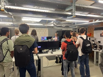
Students from Kirschgarten Gymnasium explore AFM technology at Nanosurf, gaining practical insights into nanotechnology ...
12.06.2024
10.11.2023

Héctor here, your AFM expert at Nanosurf calling out for people to share their Friday afternoon experiments. Today I'll show you how to dig using an AFM and diamond probes.
Last week for the Coherer effect post, I was very lucky and got hold of a batch of diamond probes from Adama Innovations to do electrical measurements and indentation. Apart from being good for electrical measurements, it turns out these probes are also quite resistant against abrasion, and the spring constant of their new AD-450 goes up to 450 N/m (which is quite stiff compared to the 10 - 20 N/m I regularly use). So, I asked myself, can I use these probes to dig out material and see inside of a sample?
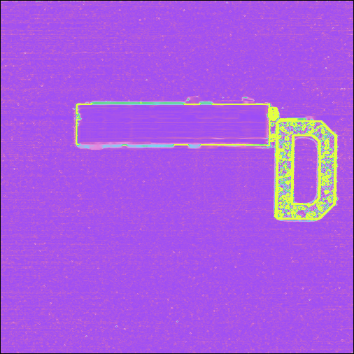
I took an old IC chip from a webcam and located 3 suitable areas for digging. The chip is from a Logitech C615 camera from the year 2015, if you have been following #fridayAFM, you might remember that I was collecting photodetector ICs to do a pixel size vs year.
The idea here is that there are structures of different material, either a metal, or doped silicon, buried underneath the silicon oxide, and each time the diamond tip pases on top, it chips away some atoms, eventually exposing the buried structures. Ok, easy said than done... how much force we applied, for how long we scan? To figure out these questions, I made a little test in areas 1 and 2.
The result on Area 1 was something like this:

Or as a summary, this is what happened:
Scanning over the structure did eroded the middle part, however, because the part was protruding above the surface, at some point the lateral force exerted by the probe started chipping away material. So, lesson here, try to dig on flat areas and reduce the lateral forces.
Once the proof of concept was tested, I moved to Area 2 and used a script that takes a few scans at a given set point, then zooms out to see the amount of digging done, then increases the setpoint and repeats.
import nanosurf
import time
import numpy as np

#Setpoint steps
sp_steps=5
sp_start=7500e-9 #in N
sp_end=8500e-9
sp_valueimaging=200e-9
repetitions_at_each_sp=5
sp_value=sp_valueimaging #Initial setpoint value

#zoom in and out steps (i.e. imaging with small setpoint)
zoom_in_steps=3
zoom_in_area=20 * 1e-6
scantime_zoom_in=0.2
points_zoom_in=500
zoom_out_area=40 * 1e-6
scantime_zoom_out=0.4
points_zoom_out=500
zoom=zoom_out_area #Initial zoom value

#Script asumes the CX software is started,
#static mode selected, laser adjusted, probe
#landed on the surface, and all probe calibrations has been done.
spm = nanosurf.SPM()
application = spm.application
scan = application.Scan
stage = application.Stage
zcontroller = application.ZController
zcontroller.SetPoint = sp_value

#Because we will change the scanning parameters several times, better to make a function
def setupAFM(sp_value,width,pixels,scantime):
        zcontroller.SetPoint = sp_value
        scan.ImageWidth = width# Set width of scan to 10 um
        scan.ImageHeight = width
        scan.Points = pixels
        scan.Lines = pixels
        scan.Scantime=scantime

#Main loops
for h in range(sp_steps+1):
    #Zoom_in_process
    for k in range(zoom_in_steps+1):
        zoom=zoom_out_area+(zoom_in_area-zoom_out_area)/zoom_in_steps*k
        setupAFM(sp_valueimaging,zoom,points_zoom_out,scantime_zoom_out)
        scan.StartFrameUp()
        # Check if scanning
        while scan.IsScanning == True:
            print("Scanning")
            time.sleep(scantime_zoom_out*points_zoom_out+scantime_zoom_out*points_zoom_out*0.1)

    #Digging
    sp_value=sp_start+(sp_end-sp_start)/sp_steps*h
    for m in range(repetitions_at_each_sp):
        setupAFM(sp_value,zoom_in_area,points_zoom_in,scantime_zoom_in)
        scan.StartFrameUp()
        # Check if scanning
        while scan.IsScanning == True:
            print("Scanning")
            time.sleep(scantime_zoom_in*points_zoom_in+scantime_zoom_in*points_zoom_in*0.1)

    #Zoom_out_process
    for k in range(zoom_in_steps+1):
        zoom=zoom_in_area+(zoom_out_area-zoom_in_area)/zoom_in_steps*k
        setupAFM(sp_valueimaging,zoom,points_zoom_out,scantime_zoom_out)
        scan.StartFrameUp()
        # Check if scanning
        while scan.IsScanning == True:
            print("Scanning")
            time.sleep(scantime_zoom_out*points_zoom_out+scantime_zoom_out*points_zoom_out*0.1)
The result is something like this:
Still working on how to process the data and show a nice video... so if you watch it, play it a twice the speed at least... Here is the summary.
This time it worked better than the previous test because the surface was "flat". By the way, what flat means? Check out how to measure the flattest surfaces on earth in our app note. From this test we also learnt that we can apply up to 100 μN before the cantilever breaks (don't know how much because it didn't broke and the photodetector max out).
Now for the buried structures. Area 3 has some of those. The question is, how are we going to check if we dig too much? Optically we could see "squares" in Area 2, yet from the AFM data is unclear if we reached them or not.
The answer is scanning microwave microscopy (SMM).
SMM sends a radio frequency signal (at about 5 GHz) down a metallic probe onto the sample and compares the outgoing signal against the reflected wave. SMM contrast reveals differences in conductivity, hence it distinguishes between conductors and insulators, and permits to judge changes in doping also (to know more about it, check out our application notes on SMM: measuring dopant density, and study of capacitance).
So, I connected the microwave system (which uses a different probe by the way, not the diamond anymore), found the resonant frequency of the cables + probe + sample... and measured the changes in microwave absorption. The result is something like this, first the digging:
and here the microwave part:
I managed to dig about 25 nm of material in a quite uniform way (the lessons learnt from areas 1 and 2 worked). However, when comparing the microwave signals before/after, there is barely any difference, thus, I conclude that the structure has to be much deeper than 25 nm (at lest so deep that 25 nm of material make no difference).
Final remarks: Diamonds are truly forever, after 3437 scans, most of them with high setpoint and fast scanning speed, the diamond probe is still going and we managed to dig quite nice holes in SiOx (up to 25 nm deep). SMM is a nice tool to investigate conductivity, here it tell us that after digging 25 nm the buried structure is likely to be much more deeper, because the SMM signal didn't change.
I hope you find it useful, entertaining, and try it yourselves. Please let me know if you use some of this, and as usual, if you have suggestions or requests, don't hesitate to contact me.
Further reading:
1 Unveiling the Power of Electrical Modes. https://web.nanosurf.com/unveiling-the-power-of-electrical-modes
12.06.2024
Students from Kirschgarten Gymnasium explore AFM technology at Nanosurf, gaining practical insights into nanotechnology ...
29.11.2023
Discover how Nanosurf's collaboration with a team of scientists has revolutionized spring constant calibration for ...

01.11.2023
Explore the evolution and diverse applications of electrical AFM modes in industries such as semiconductor technology, ...

11.07.2024
FridayAFM: learn how to perform datamining on large sets of AFM data.

02.07.2024
FridayAFM: learn how to automatize data analysis in MountainsSPIP

26.06.2024
FridayAFM: learn how AFM makes possible modern ball point pens.
Interested in learning more? If you have any questions, please reach out to us, and speak to an AFM expert.