Discover the capabilities of WaveMode AFM in characterizing bottlebrush polymers with unprecedented detail and speed, ...

15.12.2023

Héctor here, your AFM expert at Nanosurf calling out for people to share their Friday afternoon experiments. Today we will measure again the conductivity of interfaces, this time with a logarithmic current meter.
Murphy's law states that: "anything that can go wrong will go wrong".
I translated this onto a law for nanoelectrical characterization: "never measure twice, it will not work again".
Then I added Héctor's corollary: "The first run will be the best, always save it".
That is why, when I got access to the new logarithmic current sensing system, I was hesitant to repeat old measurements with it and see what benefits can I get from having a current meter that can measure through several decades of current with the same sensitivity in each range. But on the other hand, when I posted about the Coherer effect I got challenged to see more details on the part where there is tunneling current. So, Héctor's axiom took over: "never run away from a challenge".
The logarithmic current sensing system (officially called scanning spreading resistance microscopy or SSRM for short) comes with a new sample holder and its electronics packed inside of a external box that connects between the sample and the AFM driver. The setup is something like this:
I know I know, I forgot to take a picture of the resistor used to limit the current, but I think I did a good job with the CGI, didn't I?
The new sample holder is designed to be grounded on the outside and connected to the current sensing device in the inner part. This is good for samples that conduct through the substrate, for samples where the conductive element is on top of an insulating substrate I use aluminum foil around the sample, and the clamps (which are covered in Kapton tape to prevent shorting things to ground). The pressure on the aluminum foil is enough to break the oxide barrier and guarantee good conduction.
So, what are we going to measure? I have a new surface, Au on Mica, as seen in the picture, Indium Tin Oxide (ITO), as seen previously in #fridayAFM (see below almost a year ago), and I want to repeat the oxide layer measurements in aluminium oxide.
I started with the Au surface, as I expect it to be the easier to interpret, however, it was not the easiest to image. I first used a probe with a spring constant of about 40 N/m, and found that no matter how low I set the setpoint in Static mode, I was always damaging the surface. So, after a few attempts, I changed to a probe with lower spring constant and managed to take the results you can see here:
The images of the surface are nice, but not very relevant here, they are just to show that there wasn't any obvious contamination in the region. The conductivity map is presented in volts as measured by the logarithmic current meter (to convert to current one has to solve the equation show in the first figure for INUM). What is relevant are the force-distance graphs I took at random locations. Initially, these plots show deflection and the logarithmic voltage measured by the logarithmic meter, however, analyzing the results using the signal is very difficult, so I converted it to current for convenience. Also, to help visualizing things, by graying out part of the graphs, I indicated in each case the values of the current that are not accessible because the current limiting resistor is limiting the current available.
What can we learn from these measurements? Most important, of all, that we can see the transition from tunneling to ohmic (as seen in the case of 0.4 V applied to the probe), and that the rate at which current increases in the tunneling region changes with the applied voltage.
Hold on.
I though gold doesn't create an oxide barrier, and if you are using a diamond probe, why is there a tunneling current? The answer is ambient and contamination (there is also something to do with contact area, deformation, temperature... but I want to keep it simple), see for instance Ref 1 for more details.
A part from the tunneling, what else can we see? Well, we can measure how much we need to indent before obtaining an ohmic contact, about 20 nm. Hold on again, but this seems to be smaller with smaller applied voltages, what is happening? What happens is that with 0.1 and 0.2 V, we are limiting the current so much that in the tunnelling region we already reach the maximum current available and we don't get to see the transition to ohmic, and thus we cannot use those measurements to extract how much we need to indent to obtain ohmic conduction.
Time to change to the ITO sample.
In this case, again the images of the surface are nice (the voltage shows more contrast than in the #fridayAFM from 2022 12 16), but their only purpose is to show that the area is "clean".
On the ITO we can also see the transition from tunneling to ohmic, but there is something more. The contact resistance is acting as a resistor in series with the limiting resistor, and if we calculate how much is its value, we can se that about 13 kOhm fits well with the three cases presented here (of course if we have a large indentation with will change as the contact area will be larger, but for small indentations it should not change much).
Isn't it nice that on the anniversary of imaging ITO for first time in fridayAFM we can learn something new about this sample?
Now it is time for the kitchen foil again.
In this case, even with large voltages we were reaching the limiting current before seeing the transition between tunnelling and ohmic, so for the 0.8 V and 3 V measurements I removed the limiting current resistor and extended the indentation range.
What can we see? We see the transition from tunnelling to ohmic, and that this transition occurs at different indentation depth if we vary the applied voltage. Is this in accordance to our previous measurements? If you go back to the final graph in the Coherer effect, you will see that indeed it matches those results, but here, thanks to the logarithmic meter we see not just a sudden jump in current but a gradual increase as we indent.
Also, if we estimate the contact resistance, is about 20 kOhm, which is similar to the value obtained for Gold (at least it is not several orders of magnitude different).
Let's recap. The logarithmic current meter allowed to see what happens in the tunneling regime, as opposed to the linear current meter used previously that just indicated a jump in current when ohmic connection was achieved. This allowed us to look at Au, ITO and Al surfaces. Obtaining the contact resistance when indenting a few tens of nm with a diamond probe. In the case of Al, we measured the indentation to ohmic, which changed with the applied voltage, and this dependence matched our previous results pointing towards an oxide barrier of about 307 nm.
I hope you find this useful, entertaining, and try it yourselves. Please let me know if you use some of this, and as usual, if you have suggestions or requests, don't hesitate to contact me.
Conductive AFM (C-AFM) measurements on a polished IC surface with multiple transistor contacts
Unveiling the Power of Electrical Modes
Further reading:
[1] Nathan L. Tolman, Ruobing Bai, and Haitao Liu, Hydrocarbons in the Meniscus: Effects on Conductive Atomic Force Microscopy. Langmuir 2023 39 (12), 4274-4281(2023) https://doi.org/10.1021/acs.langmuir.2c03222
28.10.2025
Discover the capabilities of WaveMode AFM in characterizing bottlebrush polymers with unprecedented detail and speed, ...

27.10.2025
Read this blog and discover advanced alloy engineering and cutting-edge AFM techniques for high-resolution, ...

14.10.2025
Discover how WaveMode technology resolves the tobacco mosaic virus structure under physiological conditions with ...

08.12.2024
Learn how to make a Python code to interface your AFM with a gamepad.
01.10.2024
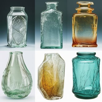
Discover how different types of glass age and degrade over time, and learn how to use AFM technology to investigate ...
11.07.2024
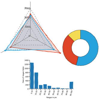
FridayAFM: learn how to perform datamining on large sets of AFM data.
Interested in learning more? If you have any questions, please reach out to us, and speak to an AFM expert.