Discover the capabilities of WaveMode AFM in characterizing bottlebrush polymers with unprecedented detail and speed, ...

25.08.2023
Héctor here, your AFM expert at Nanosurf calling out for people to share their Friday afternoon experiments. Today I return to one of my favourite topics, memory.
Flash memory chips are ubiquitous since the 80s. Not only on home computers such as the Commodore 64, but also in USB drives, memory cards, hard disk drives (yes, to store the code that makes them tick), toys that play tunes, cameras (I'm talking here about 90s cameras), televisions, and eventually, mobile phones.
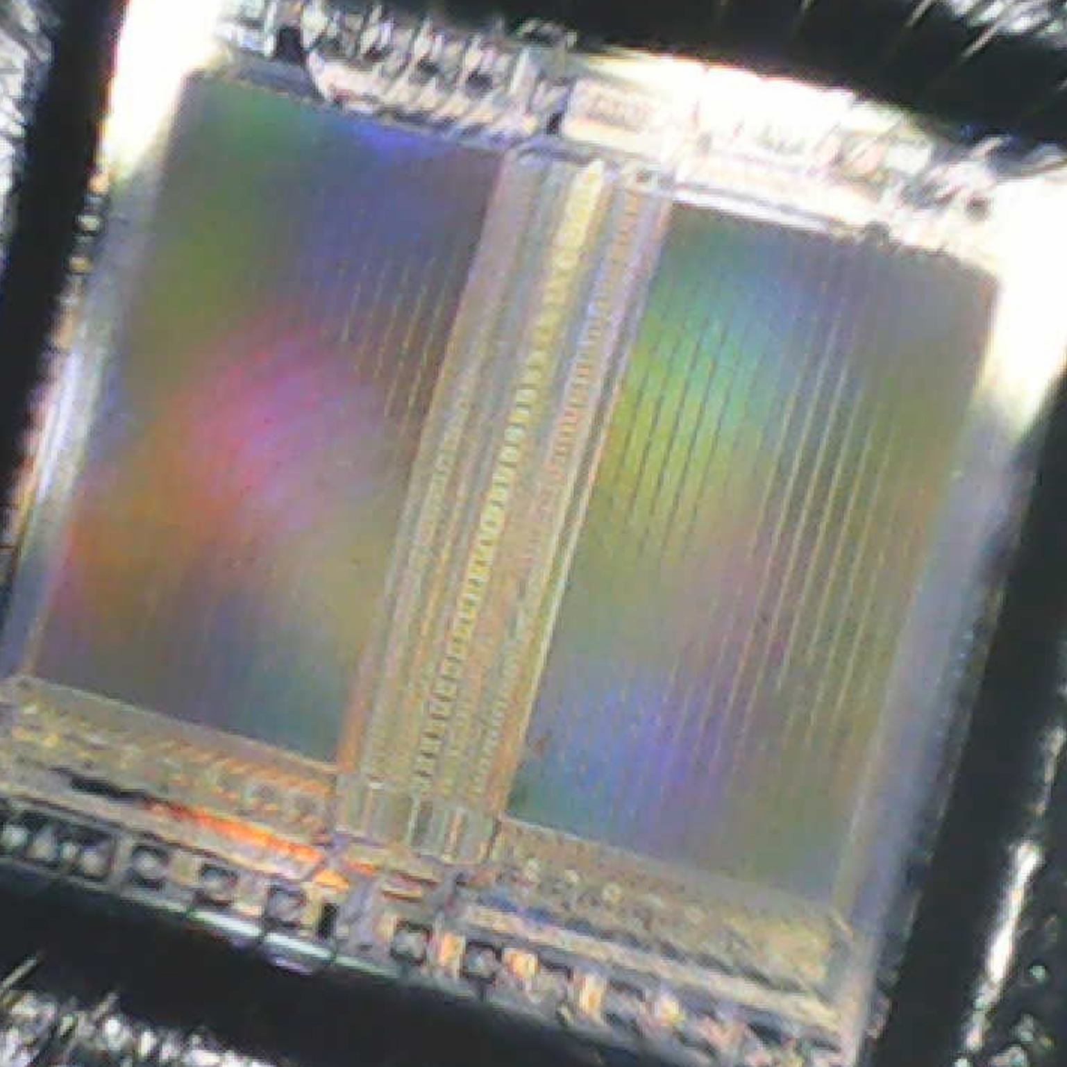
The chip I brought here today I found inside of a Kalok hard disk (which I was opening for another fridayAFM). Not sure what it does, it could act as a buffer to read/write onto the hard drive (which makes sense since it has two data banks), or it could act as a storage for the code that controls the hard disk.
Opening the encapsulation is quite easy on these UV-erasable chips, they tend to split in two without too much hassle.
Once opened, a quick inspection with the AFM optical microscope leads to a couple of surprises. First one, despite the Kalok being from 1989... the EPROM design seems to be from 1984 (this reinforces my suspicion that on this hard drive, the bottleneck to higher bit density is due to the way the read/write head is actuated, i.e. with a stepper motor rather than with permanent magnets and coils).
By the way, with the IC designation (HN27C256G according to the encapsulation, HN27C256 according to the die) it is easy to obtain the spreadsheet and details about the chip. It is indeed an EPROM, UV erasable, and once multiplied, the 32768 times 8 bit give us 262144 bits, or 256K.
With the chip open and mounted onto the AFM, and with enough space for the AFM probe to reach almost every corner, I proceeded to take some topography images. The next two images, which are several AFM scans stitched together, show how the memory elements interface with the word and bit decoding structures respectively.
I have absolutely no idea what we see in the decoding area, and couldn't find references for it (other than that the memory is arranged in an array in rows and columns), but the memory element is likely to have the elements highlighted in the diagram. However, the structure I show in the next image is just a guess, based on the visible elements and the requirements of a floating-gate transistor (the "empty" space between elements is supposed to be filled with an insulating barrier).
My guess regarding the transistor shape is based on the fact that the memory elements have a bump in the middle (maybe indicating the pilar going up from the source), and the requirement for the transistor to have three terminals (drain source and gate). In this case, when a voltage is applied to the word line, depending on the charge on the floating gate, it will create an electric field between the bit line and the source pilar that enables (or restricts, depending on the floating gate) the flow of electricity.
So... If the guess with regards to the transistor structure is correct, it means that by measuring surface potential (i.e. doing KPFM), we might be able to see the floating gates, if they still hold any charge.
Ignore the yellow line-shaped signal at the edge of each memory element. It is likely to be either part of the insulation at a much different surface potential, or an artefact due to tip-sample interaction.
From the values of the surface potential (uncalibrated), there is a spread in the potential seen at the centre of the memory elements, which spans from 1.8 to 4V. From a quick glance it is not possible to see a clear division, but if we plot a histogram of the values...

It is clear that there is a gap around 3.3 V, this allow us to categorize the memory elements into two values (i.e. "0" and "1").
So... yes we can retrieve data from this 30+ year old memory device. This also reinforces the argument that this is a pseudo-static random memory, more precisely, a NOR flash memory (the bit line interfaces directly with the memory elements). This is important, because if it were a static memory, it would take four elements to store one bit, while a pseudo-random uses only one. It is critical to establish this point, because of how it compares to our previous fridayAFM. It is curious that as of bit density, this EPROM has smaller bits than a chip from 1985... but they are from different companies... so it is possible that they were using different fabrication processes.
By the way, I hope to fill this plot with more data points in the future, so... stay tuned.
Here it is the previous fridayAFM on another EPROM (also from another hard disk drive).
I hope you enjoyed what I showed you. Stay in touch, and if you have more info, please share (especially if you have information related with the transistor internal geometry).
... and if you made it this far, here are some discarded images.
28.10.2025
Discover the capabilities of WaveMode AFM in characterizing bottlebrush polymers with unprecedented detail and speed, ...

27.10.2025
Read this blog and discover advanced alloy engineering and cutting-edge AFM techniques for high-resolution, ...

14.10.2025
Discover how WaveMode technology resolves the tobacco mosaic virus structure under physiological conditions with ...

08.12.2024
Learn how to make a Python code to interface your AFM with a gamepad.

01.10.2024
Discover how different types of glass age and degrade over time, and learn how to use AFM technology to investigate ...
11.07.2024
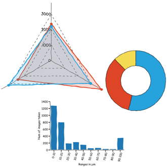
FridayAFM: learn how to perform datamining on large sets of AFM data.
Interested in learning more? If you have any questions, please reach out to us, and speak to an AFM expert.