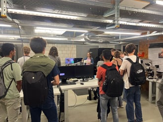
Students from Kirschgarten Gymnasium explore AFM technology at Nanosurf, gaining practical insights into nanotechnology ...

12.06.2024
The ultimate tool for nanoscale research from biological molecules to advanced new materials.
The versatile mid-range research AFM that grows with your demands in modes and accessories.
A compact affordable research AFM that is astoundingly easy to use, with more than 30 modes and options.
Measure roughness and other material properties of heavy and large samples up to 300 mm and 45 kg.
Bringing the power of DriveAFM to a wafer metrology system purpose-built for the requirements of the semiconductor industry.
For unique requirements, we will design a bespoke AFM solution, leveraging our decades of engineering expertise.
Slide an AFM onto your upright optical microscope turret for a leap in resolution.
One of the smallest ever AFMs, created for integration into custom stages or existing setups.
A flexibly mountable research-grade scan head for integration into custom stages or existing set ups.
What is atomic force microscopy (AFM)? How does AFM work? What AFM modes do I really need? How do I get started with AFM?
Learn how AFM works with cantilever/tip assembly interacting with the sample. Explore CleanDrive technology, calibration methods, and feedback principles for precise nanoscale imaging.
An overview of common AFM modes. To learn about each mode in more detail and see application, view the full article.
We regularly publish detailed reviews providing practical guidance and theoretical background on various AFM applications.
Read detailed technical descriptions about selected AFM techniques and learn how to perform specific measurements on Nanosurf instruments.
A library of links to research papers in which Nanosurf instruments were used.
Learn AFM from our library of recorded webinars, covering different measurement techniques, modes, and areas of application.
Short video clips explaining how to perform different operations on Nanosurf instruments.
Watch a product demonstration to learn about the capabilities of our AFMs.
Short videos of our AFMs.
Browse news articles, press releases and a variety of other articles all around Nanosurf.
Browse Héctor Corte-Léon's weekly experiments, for inspiration, entertainment, and to discover everyday applications of AFM.
Héctor here, your AFM expert at Nanosurf calling out for people to share their Friday afternoon experiments. Today I bring you some yeast.
My background is in materials science, spintronics to be precise, hence when dealing with biological samples I'm totally out of my element (that's why I make more mistakes than usual). So, if you find mistakes, please let me know, and I will be happy to learn something new. Saying this, not having a suitable sample to try things and learn has been holding me back from increasing my experience with biological samples. Or at least until now.
Humanity has been using yeast for at least 5.000 years to prepare bread and produce alcohol (https://en.wikipedia.org/wiki/Yeast), and in this long time we have learnt many things, not only how to produce new strains (there are literally hundreds of strains of yeast dedicated to different beers), but also we have learnt how to pack yeast for long storage and ease of use.
So, if I use off-the-shelf baker's yeast, can it be an easy-to-prepare sample for AFM?
I have to add that the sugar is not paid publicity, I wanted to show that apart from the glass slides (check here how to properly clean glass slides cheaply or with expensive chemicals), all the products can be found on-the-go, and don't require a specialized laboratory for preparation.
Note that the droplets are massive in comparison to the area covered by AFM imaging, so results might vary depending on which part of the droplet is being imaged.
It worked like a charm. Ok, ok, in the first two or three images I picked up some contamination and the scan has unstable lines... but moving away from those areas and finding a nice place to scan was easy. Interestingly, this is the type of sample where the interesting stuff is hidden by the overall topography, thus flattening is needed. The "trick" I use here is that I get the topography channel, I smooth it out with a filter, leaving only the large features, and then I subtract the result from the initial image. The final product are images (in pink) that clearly show the surface features.
Now, before discussing a bit the surface features, maybe it is worth introducing the yeast life-cycle. Basically there are three types of cells which reproduce asexually, but there are ways in which one cell can turn into others, for example, by pairing, or producing spores.
From the images I took, I don't think I have seen spores been formed, or haploid cells in the process of merging onto a diploid, but I think I did pick up budding scar tissue, and more interesting, some strange surface texture in some of the cells.
From the literature research I did, I couldn't see similar AFM images, neither SEM. The closest I could find refers to dormant spores (“Towards a Nanoscale View of Microbial Surfaces Using the Atomic Force Microscope” Verbelen C. et al. Applied Scanning Probe Methods IX pp 111–126 (2008)) or yeast engineered to have hydrophobin protein on its surface to increase its viability in air and increase its range of viable temperatures (“Surface display of HFBI and DewA hydrophobins on Saccharomyces cerevisiae modifies tolerance to several adverse conditions and biocatalytic performance” Andreu C. et al. Applied Microbiology and Biotechnology volume 105, pages1505–1518 (2021)).
So... unless somebody steps up with an answer (please do so), I have no idea what I'm looking at. Is this normal in yeast? (or in this type of yeast at least). Some short of wall functionalization that happens in all types of yeast previous to spores formation in order to increase survival rate in air? Are these cells whose cell wall has been damaged? (Maybe water evaporation in bare glass is faster/slower than in Au, or surface charge of the substrate induces cell modifications). Or is it that this yeast has been engineered to have these ridges on its surface?
Hopefully, these, and some more questions that I will keep to myself, will be answered in future fridayAFM experiments (or maybe you know and are willing to share the knowledge?). The important thing for now is that this is a useful test sample and now you (and I) know how to prepare it and what images of it might look like.
Stay in touch, and share images if you try to replicate it.
Extra:
Some high resolution images for those who made it this far.

12.06.2024
Students from Kirschgarten Gymnasium explore AFM technology at Nanosurf, gaining practical insights into nanotechnology ...

29.11.2023
Discover how Nanosurf's collaboration with a team of scientists has revolutionized spring constant calibration for ...

16.10.2023
Discover how Dr. Nitya Nand Gosvami and his team at IIT Delhi harnessed the power of Nanosurf's FlexAFM and DriveAFM ...

08.12.2024
Learn how to make a Python code to interface your AFM with a gamepad.

01.10.2024
FridayAFM: learn how the extreme sensitivity of AFM can reveal the glass ageing process.

11.07.2024
FridayAFM: learn how to perform datamining on large sets of AFM data.
Interested in learning more? If you have any questions, please reach out to us, and speak to an AFM expert.
